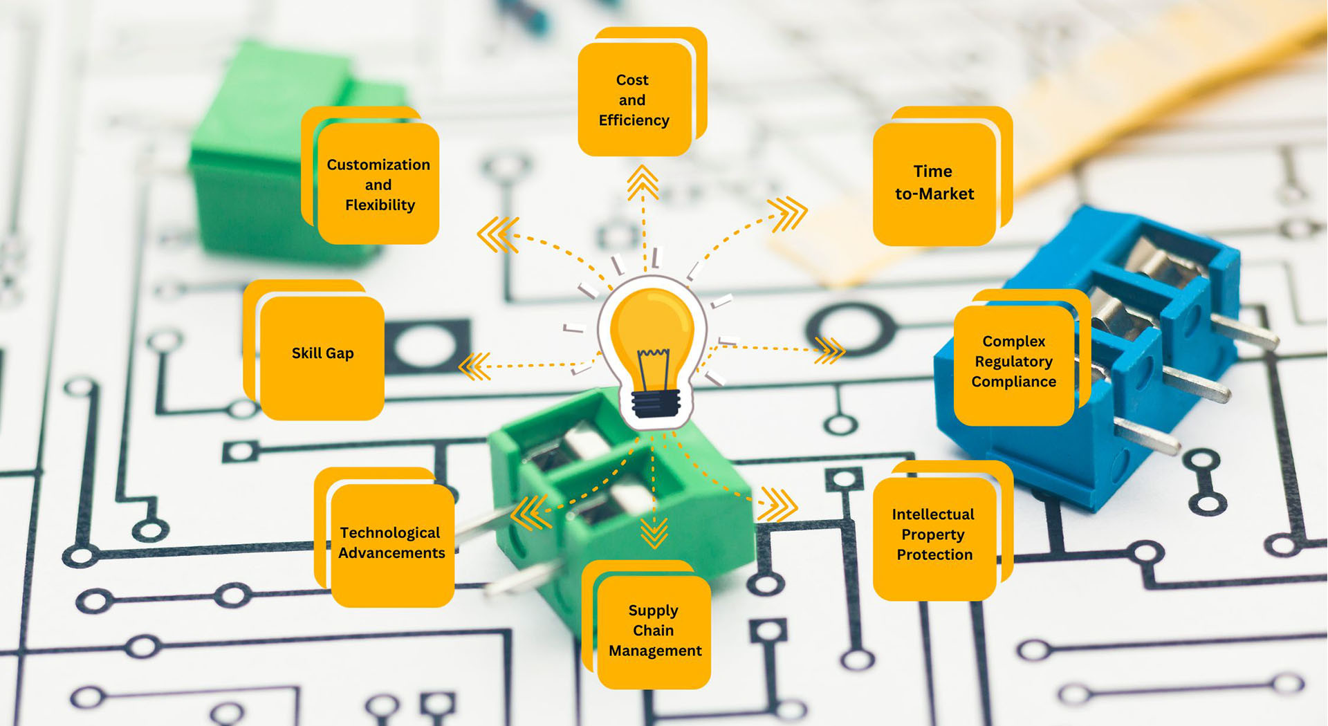

10 Important Factors to Consider When Selecting a Sensor or IoT Device
2024-06-26
The world of technology is rapidly advancing, and one of the most transformative developments is the Internet of Things (IoT). IoT applications span across various industries, from smart homes and cities to precision agriculture and industrial automation. At the core of any IoT implementation are sensors and IoT devices. These components collect essential data, enabling IoT systems to function seamlessly.
In this blog post, we will delve into the importance of selecting a sensor or IoT devices for your project. Making informed choices is critical for the success of any IoT venture. We will explore ten essential factors that engineers and IoT enthusiasts must consider when choosing sensors. These factors will help you make sound decisions, ensuring that your IoT project is not only functional but also efficient, reliable, and cost-effective.
Understanding IoT Sensors
Before we dive into the factors to consider when selecting a sensor for IoT applications, it’s crucial to understand the role of IoT sensors and their diversity. IoT sensors are devices that detect and measure physical properties such as temperature, pressure, motion, light, or environmental conditions. They are the eyes and ears of IoT systems, capturing data that drives decision-making and automation.
IoT sensors come in various types, each suited for specific applications. For instance, temperature sensors are commonly used in climate control systems, while motion sensors are vital for security and automation. The significance of understanding these differences is that making the right choice can significantly impact the performance of your IoT solution.
10 Important Factors to Consider When Selecting a Sensor or IoT Device
Factor 1: Sensor Type
The first factor to consider when selecting a sensor for your project is the type of sensor that best suits your application. Different IoT applications require various sensor types, each designed to excel in a particular area. Here, we’ll explore the most common sensor types and their respective applications.
Temperature Sensors: These sensors measure temperature and are used in climate control systems, weather stations, and cold chain management.
Pressure Sensors: Pressure sensors are vital in applications like industrial automation, tire pressure monitoring systems, and weather forecasting.
Motion Sensors: Motion sensors detect movement and are used for security, lighting control, and occupancy sensing.
Light Sensors: Light sensors measure light intensity and are essential in display brightness control, street lighting, and photography.
Environmental Sensors: These sensors monitor environmental parameters such as humidity, air quality, and radiation levels, making them invaluable in smart cities and environmental monitoring.
Matching the sensor type to your specific IoT application is crucial to ensure that your project functions optimally.
Factor 2: Sensor Accuracy
Sensor accuracy is one of the paramount factors when selecting a sensor for an IoT project. The accuracy of sensor data is fundamental in ensuring the reliability and effectiveness of the entire system. Whether the project involves monitoring environmental conditions, tracking assets, or measuring energy consumption, precise and accurate sensor measurements are imperative for meaningful data analysis and informed decision-making.
Accurate sensor data serves as the foundation upon which actionable insights are built. The value of IoT projects lies in their ability to collect and process data to derive insights that can drive improvements and efficiencies. Inaccurate sensor data can lead to incorrect conclusions and misguided actions, potentially rendering the entire IoT project ineffective.
To select sensors with the right level of accuracy, engineers must comprehend how to assess and compare sensor accuracy metrics. Sensor datasheets provide specifications such as resolution, precision, error rates, and calibration methods. Engineers need to interpret these metrics to evaluate sensor accuracy effectively.
Calibration plays a significant role in achieving and maintaining sensor accuracy. Calibration involves the process of adjusting and fine-tuning sensors to ensure their measurements are as accurate as possible. This can be performed during the sensor manufacturing process or on-site in the field. In some cases, compensation techniques may also be employed to mitigate inaccuracies and drift in sensor measurements, allowing for ongoing accuracy even in changing conditions.
Applications vary in terms of the accuracy requirements for sensor data. Some applications, like medical devices or aerospace systems, demand extremely high precision. In contrast, other applications, such as monitoring room temperature, may tolerate lower precision. Engineers must weigh the specific accuracy needs of their IoT projects against the associated costs of higher-precision sensors.
Maintaining sensor accuracy over time can be challenging, as various factors can affect sensor performance. Environmental conditions, aging, and external interferences can introduce inaccuracies. Engineers need to consider these challenges and develop strategies for maintaining accuracy over the sensor’s operational lifespan.
Cost is another critical factor when addressing sensor accuracy. High-precision sensors often come with a higher price tag. Engineers must carefully balance their budget constraints with the accuracy requirements of their IoT projects. This means making informed decisions regarding the necessary level of accuracy to achieve project goals without overspending on sensor technology.
Factor 3: Power Consumption
IoT sensors are often deployed in remote or battery-powered devices. As such, power consumption is a critical factor to consider when selecting a sensor for your project. High power consumption can lead to frequent battery replacements, increased maintenance costs, and potential downtime.
It’s essential to select sensors that are power-efficient and optimized for low energy consumption. Low-power sensors extend the lifespan of battery-operated IoT devices and reduce the overall operational cost. Engineers can choose from a wide range of sensors designed specifically for low power consumption, making them suitable for long-term, autonomous deployments.
Factor 4: Connectivity Options
IoT sensors are integral components of interconnected systems, and their connectivity options play a pivotal role in data transmission. Choosing the right connectivity solution depends on various factors, including the distance over which data needs to be transmitted, the amount of data, and power efficiency.
There are several connectivity options available, each with its advantages and limitations:
Wi-Fi: Wi-Fi offers high-speed data transmission but consumes more power. It’s suitable for applications with easy access to power sources.
Bluetooth: Bluetooth is ideal for short-range communications and is commonly used in wearable devices and smart home applications.
Cellular: Cellular connectivity provides broad coverage but requires more power and is suitable for applications with remote or mobile devices.
LPWAN (Low Power Wide Area Network): LPWAN technologies like LoRa and Sigfox are designed for long-range, low-power communication, making them suitable for applications with low energy budgets.
Selecting the right connectivity option depends on the specific requirements of your IoT project.
Factor 5: Data Rate and Throughput
The amount of data generated and transmitted by IoT sensors varies widely among applications. Some IoT systems require high data rates, while others operate with minimal data throughput. Understanding the data requirements of your project is vital when choosing sensors.
IoT applications like video streaming and real-time monitoring demand high data rates. In contrast, applications like environmental monitoring or asset tracking may require lower data throughput. Selecting a sensor for your project with the appropriate data rate capabilities ensures that your IoT system efficiently handles data transmission and processing.
Factor 6: Environmental Considerations
Environmental conditions have a significant impact on sensor selection. IoT projects can be deployed in diverse settings, from controlled indoor environments to harsh outdoor conditions or industrial facilities. Selecting a sensor that can withstand and perform optimally in the intended environment is crucial.
We’ll discuss the impact of environmental factors on sensor selection and provide guidance on choosing sensors that can endure and deliver reliable data in challenging conditions.
Factor 7: Cost
One of the primary concerns when selecting a sensor for IoT projects is cost. Balancing sensor quality with budget constraints is essential. In this section, we’ll delve into strategies for identifying cost-effective sensor options without compromising essential functionalities.
Discussing the factors that influence the cost of sensors, including sensor type, accuracy, and additional features. Offering insights into how these factors can be evaluated to make cost-effective choices.
Highlighting the importance of comparing different sensor vendors and their pricing. Offering tips on researching reputable vendors and making informed decisions based on cost and sensor performance.
Factor 8: Power Supply
Exploring the various power supply options for IoT sensors. This section will cover the essential aspects of powering sensors, including battery life, energy harvesting, and external power sources. Readers will gain insights into the trade-offs associated with each power supply option.
Discussing the significance of battery life in IoT sensor devices. Providing recommendations on selecting a sensor that offer a balance between power consumption and extended battery life. This section will also cover tips for conserving power when using battery-powered sensors.
Introducing readers to energy harvesting technologies, such as solar cells and kinetic energy harvesting. We’ll discuss the potential of energy harvesting to power sensors efficiently and its impact on sensor selection.
Factor 9: Sensor Calibration and Maintenance
Sensor calibration is a critical factor in ensuring accurate data collection. This section will emphasize the importance of calibration for maintaining sensor accuracy and reliability. We’ll explain the calibration process and how it impacts data quality.
Readers will learn the importance of sensor maintenance to ensure long-term functionality. Providing practical tips and best practices for maintaining sensors, including regular checks, cleaning, and calibration schedules. We’ll discuss how proper maintenance contributes to the longevity of IoT sensor devices.
Introducing readers to the tools and resources available for sensor calibration and maintenance. Explaining how these tools can aid engineers and users in ensuring sensors perform optimally throughout their lifespan.
Factor 10: Sensor Integration
The tenth factor, sensor integration, is crucial for the successful implementation of IoT devices. It involves the strategies and considerations for seamlessly incorporating sensors into IoT devices, ensuring compatibility with microcontrollers, and managing the data processing aspect.
This section will explore various strategies for integrating sensors into IoT devices. It will discuss considerations such as physical placement, connection interfaces, and communication protocols. Readers will gain insights into how the choice of integration methods can impact the overall performance and functionality of IoT systems.
Discussing the importance of ensuring compatibility between selected sensors and the microcontrollers or processing units used in IoT devices. Readers will learn how to identify sensors that can communicate effectively with specific microcontrollers, minimizing integration challenges.
Exploring the data processing aspect of sensor integration, including data collection, transmission, and storage. Discussing the role of IoT platforms and data management systems in handling the information generated by sensors. Providing tips on selecting a sensor that align with the data processing capabilities of the IoT ecosystem.
Highlighting the significance of testing and validating the integrated sensor systems. Readers will gain insights into the testing procedures and protocols necessary to ensure that integrated sensors function as intended. This section will emphasize the role of testing in identifying and resolving integration issues.
Addressing the scalability of sensor integration to accommodate future expansions or upgrades in IoT projects. Discussing the concept of future-proofing IoT devices by selecting a sensor that can adapt to evolving technology and application requirements.
The Role of PCB Design in Sensor Integration
Significance of PCB Design
Highlighting the role of PCB (Printed Circuit Board) design in IoT sensor integration. Effective PCB design ensures that sensors are seamlessly incorporated into your IoT devices, facilitating accurate data collection and efficient communication.
Optimizing PCB Layout
Discussing how a well-structured PCB layout can enhance sensor performance and minimize interference. Providing insights into best practices for PCB design to accommodate sensors while maintaining signal integrity.
IoT Device Miniaturization
Exploring how PCB design plays a crucial role in compact IoT devices, ensuring sensors are placed optimally for efficient use of space. Discussing how miniaturization impacts sensor selection and placement.
PCB Manufacturing Considerations
Addressing considerations when selecting a PCB manufacturer for your IoT devices. Factors such as quality, cost, and lead times can affect sensor integration.
Conclusion
As we conclude this blog post, we’ll summarize the key takeaways from the ten factors to consider when selecting a sensor or IoT devices. We’ll reinforce the importance of informed sensor selection in ensuring the success of your IoT project. Finally, we’ll touch on the promising future of IoT and the pivotal role that sensors will continue to play in shaping that future.
Stay tuned for the complete blog post, where we’ll explore each of these factors in greater detail, providing engineers and IoT enthusiasts with valuable insights into the art of selecting the right sensors for their projects.
View More
Excellence Quality Assurance: The Secrets of High-Quality PCB Manufacturing
2024-06-26
Printed Circuit Boards (PCBs) are the backbone of countless devices we use daily. From smartphones to industrial machinery, PCBs are the essential electrical connection conduit. However, the efficiency and reliability of these devices heavily rely on the quality of PCB manufacturing.
Quality Assurance (QA) is not just a step in the process; it’s a commitment to excellence that permeates every aspect of production. In this blog, we’ll delve into the pivotal role of QA in PCB manufacturing, exploring the top nine secrets that ensure the production of high-quality PCBs. From circuit board design optimization to team collaboration, each element plays a crucial role in achieving excellence in PCB manufacturing.
Understanding the Importance of Quality Assurance
Quality assurance in PCB manufacturing is not merely a checkbox; it’s a fundamental principle that underpins the entire process. Ensuring high-quality PCBs enhances product reliability and reduces the likelihood of costly recalls and repairs, safeguarding reputation and revenue.
A robust QA system encompasses stringent standards, meticulous testing, and proactive problem-solving. It involves every manufacturing stage, from PCB layout design to final inspection, fostering a culture of excellence and accountability.
Top 9 Secrets of Manufacturing High-quality PCBs
1. Understanding Design Optimization and DFM
The journey towards high-quality PCBs begins with meticulous PCB layout design. Design for Manufacturability (DFM) principles should be integrated to streamline the manufacturing process and minimize potential errors.
This involves optimizing component placement, trace routing, and ensuring adequate clearance and spacing. PCB layouting is not just about arranging components. It is about creating an efficient, manufacturable design that maximizes performance and reliability.
Talking about trace routing is crucial in optimizing the PCB layout. Efficient routing involves establishing clear pathways for electrical signals while minimizing signal interference and ensuring signal integrity. Careful attention to routing can help reduce signal delays, improve signal quality, and enhance overall system performance.
2. Choosing the Right Supplier
Selecting a reliable PCB manufacturer is paramount. Look for suppliers with a proven track record of quality and reliability. Consider factors such as manufacturing capabilities, adherence to industry standards, and customer feedback. Collaborating with a trusted partner ensures consistency and excellence in every batch of PCBs.
A reliable supplier is not just a vendor but a strategic partner invested in your success. Other than PCB suppliers, components suppliers are crucial to the PCB assembly product’s final quality.
Pay close attention to customer feedback and reviews when evaluating potential suppliers. Insights from other clients can provide valuable insights into the supplier’s reliability, responsiveness, and overall customer satisfaction.
Look for testimonials and case studies highlighting the supplier’s ability to meet deadlines, promptly address concerns, and maintain open communication throughout manufacturing.
3. Component Placement and Ideal Alignment
Component placement and ideal alignment are not merely procedural steps in the manufacturing process; they are foundational pillars upon which the entire functionality and reliability of electronic systems rest. This critical aspect of engineering demands meticulous attention to detail and an understanding of the intricate interplay between components.
In the realm of PCB layout design, achieving precise component placement stands as a linchpin for optimal performance and unwavering reliability. It’s akin to orchestrating a symphony, where each instrument must be positioned with precision to harmonize seamlessly and produce a flawless melody. Similarly, in electronics, every component must find its rightful place on the PCB (Printed Circuit Board) design to ensure smooth operation and efficient functionality.
4. Keep Soldering Temperature and Time in Check
Soldering is a critical process that demands precision and control. Maintaining the correct soldering temperature and duration is essential to prevent defects such as cold joints, solder bridges, and component damage. Employing advanced soldering techniques and monitoring equipment ensures uniform soldering and adherence to quality standards.
Advanced soldering techniques, such as the use of soldering irons with precise temperature control or reflow ovens for surface-mount components, provide the necessary precision to meet stringent quality standards.
Additionally, employing monitoring equipment, such as thermocouples or infrared cameras, allows real-time monitoring of soldering temperatures, enabling prompt adjustments to ensure optimal conditions throughout the process.
5. Use Premium Quality Flux
Flux plays a vital role in soldering by promoting wetting and preventing oxidation. Opt for high-quality flux compatible with the soldering process and materials used. Quality flux enhances solderability, improves joint strength, and reduces the risk of defects such as voids and cracks. Investing in premium flux is not just a cost; but also an investment in the reliability and longevity of your PCBs.
By prioritizing quality over cost-cutting measures, manufacturers can mitigate the risk of solder-related defects and ensure the consistent performance of their electronic devices. In the long run, the benefits of using premium flux far outweigh the initial investment, leading to enhanced product reliability, reduced rework, and, ultimately, greater customer satisfaction.
6. Use Proper ESD Protection
Electrostatic discharge (ESD) poses a significant threat to PCBs during manufacturing and assembly. Implement proper ESD protection measures to safeguard sensitive components and circuits from damage. This includes using antistatic workstations, grounding straps, and ESD-safe packaging throughout production.
ESD-safe packaging is essential for transporting and storing sensitive electronic components and PCBs. ESD-safe packaging materials, such as conductive foam and static-shielding bags, protect against external static charges and prevent damage during transit and storage.
7. Perform Inspection Processes
Regular inspection is a cornerstone of quality assurance in PCB manufacturing. Conduct thorough visual inspections, automated testing, and functional testing at every stage of production. Identify and rectify any anomalies or defects promptly to maintain the highest standards of quality and reliability.
Manufacturers can identify and rectify defects early by performing comprehensive inspection processes throughout the production cycle, minimizing the risk of defective products reaching the market. This proactive approach enhances product quality and reliability, reduces rework costs, and improves overall manufacturing efficiency.
8. Focus on Team Collaboration
Effective collaboration among stakeholders is key to achieving excellence in PCB manufacturing. Foster open communication and teamwork between design engineers, production staff, and quality control personnel. Encourage knowledge sharing, feedback loops, and continuous improvement initiatives to optimize processes and enhance product quality. Qualified workers operate and implement as per the SOP(Standard Operation Procedure), which also plays a crucial role in the final product quality.
9. Tracking and Analysing Data
Data-driven insights are invaluable for continuous improvement and quality optimization. Implement robust data tracking and analysis systems to monitor key metrics such as defect rates, yield rates, and process efficiency.
Use this data to identify trends, diagnose issues, and implement corrective actions that drive quality and productivity improvements. Data analysis is about crunching numbers and gaining actionable insights that inform decision-making and empower your team to deliver exceptional results.
Final Thoughts
The quest for high-quality PCBs is an ongoing journey fueled by innovation, collaboration, and a relentless pursuit of excellence. By embracing the secrets of manufacturing outlined above and prioritizing quality assurance at every step, manufacturers can deliver PCBs that meet the highest standards of performance, reliability, and customer satisfaction.
Quality is not just a metric. It’s a mindset—a commitment to craftsmanship and integrity that defines the very essence of PCB manufacturing.
Silk Road aspires to continue raising the bar, upholding the principles of excellence, and propel the industry forward into a future where high-quality PCBs power innovation and inspire confidence in every device they inhabit.
View More
Top 7 Tips for Creating a Reliable Embedded System with a Focus on PCBs
2024-06-26
In the rapidly advancing world of electronics, embedded systems have become the cornerstone of countless innovations, driving everything from smart devices to industrial automation. Ensuring the reliability of these embedded systems is not just a choice; it’s a necessity. In this blog post, we will explore seven invaluable tips for creating a reliable embedded system, with a special focus on the role of Printed Circuit Boards (PCBs).
Understanding Embedded Systems
Before delving into the tips for reliability, let’s establish a common understanding of what embedded systems are and their significance in today’s electronic landscape. Embedded systems are specialized computing systems that are dedicated to performing specific tasks. They can be found in a wide range of applications, including consumer electronics, automotive systems, medical devices, and industrial automation.
The Role of PCBs in Reliable Embedded System
Printed Circuit Boards (PCBs) are the silent conductors that orchestrate the flow of electricity in embedded systems, ensuring that components and subsystems work in harmony. PCBs in Embedded Systems play a profound role in their reliability and performance.
Component Interconnections: PCBs serve as the central hub where all system components are interconnected. Components such as microcontrollers, sensors, memory, and power management units are mounted on the PCB and interconnected through traces and vias. The PCB layout must be meticulously designed to facilitate these connections and minimize signal interference.
Power Distribution: PCBs are responsible for efficiently distributing power to all components within the system. Properly designed power planes, coupled with careful consideration of voltage regulation and protection, are fundamental in ensuring that components receive clean and stable power. Inadequate power distribution can lead to component instability and potential damage.
Signal Routing: PCBs handle the routing of signals between components. Effective signal routing is critical for maintaining signal integrity and preventing interference or noise. The PCB layout must consider trace lengths, impedance matching, and avoiding cross-talk to ensure reliable signal transmission.
Thermal Management: Heat management is an essential function of PCBs in Embedded Systems. Components generate heat during operation, and PCBs can be designed to efficiently dissipate this heat. Strategies like using thermal vias, heat sinks, or even copper pours can help in dissipating heat away from sensitive components, preventing overheating that could degrade performance and reliability.
Component Placement: The strategic placement of components on the PCB is crucial for achieving system reliability in PCBs for Embedded Systems. Components sensitive to noise or interference should be isolated from potential sources of disruption, while components that need to communicate with each other should be situated close together. Component placement impacts signal integrity and overall system performance.
PCB Design Tools: The design of reliable PCBs benefits from the use of specialized PCB design tools and software. These tools offer features such as design rule checks (DRC) to ensure that the design adheres to industry standards. Additionally, they may provide simulation capabilities to analyze factors like signal integrity and thermal performance.
Prototyping: Before full-scale production, creating a prototype of the PCB design is a wise practice. Prototyping allows designers to validate the design’s functionality, verify that it meets the system’s requirements, and identify any potential issues that could affect system reliability. It provides an opportunity to address and correct design flaws early in the development process.
Documentation: PCB design is heavily reliant on documentation. Detailed design specifications, schematics, and layout information are necessary for understanding and modifying the design. Comprehensive documentation ensures that others involved in the system’s life cycle can effectively manage, troubleshoot, and maintain the PCB.
Tip 1: Careful Component Selection
Creating a reliable embedded system begins with meticulous component selection. Here’s a more detailed exploration of this tip:
Component Compatibility: The key to selecting components for your embedded system is ensuring their compatibility with the system’s requirements. Each component should fall within specified operating parameters, including temperature ranges, voltage levels, and ESD protection. For instance, if you’re designing an embedded system for automotive applications, components should be rated to withstand the extreme temperature variations and automotive voltage levels.
Risk Assessment: Conduct a thorough risk assessment to identify potential weak points in component selection. Consider the implications of using components that don’t meet the system’s requirements. For example, if a component isn’t ESD-protected and your application is in an environment with a high risk of electrostatic discharge, you risk component damage and system failure.
Vendor Reputation: Consider the reputation of component vendors. Established vendors with a history of delivering high-quality, reliable components are often a safe choice. Their components are more likely to adhere to industry standards and exhibit consistent performance.
Cost vs. Reliability: Striking a balance between cost-effectiveness and reliability is essential. While you don’t want to overspend on over-specified components, cutting costs by selecting unreliable or subpar components can result in failures, costly replacements, and damage to your system’s reputation.
Lifecycle Considerations: Assess the lifecycle of components, especially if your embedded system is intended for long-term use. Ensure that the components you choose will remain available for the foreseeable future to support maintenance and repairs.
Component selection is the foundation of creating a reliable embedded system. Inadequate or incompatible components can lead to system failures and costly consequences. Careful consideration, risk assessment, and compatibility checks ensure that your chosen components align with the system’s requirements and long-term reliability.
Tip 2: Thorough PCB Design
A well-thought-out PCB design is vital for creating a reliable embedded system:
Signal Integrity: Ensuring signal integrity is crucial for reliable embedded systems. Minimizing noise and interference is key to this. Proper PCB design practices, including careful component placement, routing, and ground and power plane management, help maintain signal integrity. Signal integrity issues can lead to data corruption, system crashes, and malfunctions.
Component Placement: Placing components on the PCB strategically is important. Component placement can affect the performance and reliability of your system. For example, components sensitive to noise or interference should be placed away from potential sources of disruption, while components that need to communicate with each other should be close together.
Design Rule Checks: Utilizing PCB design tools, you can implement design rule checks (DRC) to ensure that your design adheres to industry standards and best practices. DRCs help identify issues like spacing violations, unconnected nets, or incorrect pad sizes, reducing the risk of design errors.
PCB Design Tools: Modern PCB design tools offer a range of features to aid in designing reliable PCBs. These tools may include simulation capabilities, auto-routing for efficient trace layout, and libraries of components to streamline the design process.
PCB Prototyping: Consider creating a prototype of your PCB design before full-scale production. Prototyping allows you to verify that the design functions as intended and to identify any potential issues that could affect system reliability.
PCB design is a critical component in the reliability of your embedded system. Proper design practices help mitigate noise, interference, and other factors that can compromise system performance. By following design best practices and using PCB design tools, you can enhance the reliability of your embedded system.
Tip 3: Robust Power Management
Efficient power management is crucial for the reliability of an embedded system. Here’s a closer look at this tip:
Voltage Regulation: Implementing robust voltage regulation is essential to ensure that components receive the correct voltage levels, preventing under-voltage or over-voltage conditions that can damage components or lead to system failures.
Protection Circuits: Including protection circuits such as over-current protection and over-voltage protection can safeguard your embedded system against external events, like power surges or voltage spikes, which can be detrimental to system reliability.
Power Distribution: Efficient power distribution on the PCB ensures that power is delivered to components without noise or interference. Proper power plane management, including minimizing voltage drop, is crucial for reliable power distribution.
Thermal Considerations: Power management is also tied to thermal considerations. Components that generate excessive heat may require additional measures for effective heat dissipation. Overheating can impact the reliability and lifespan of components.
Energy Efficiency: In addition to power management, energy efficiency is increasingly important for both environmental reasons and system reliability. Reducing power consumption not only saves energy but also minimizes the heat generated within the system.
Robust power management is fundamental to the reliability of embedded systems. Proper voltage regulation, protection, and efficient power distribution on the PCB are critical for preventing issues related to power fluctuations and thermal management.
Tip 4: Effective Heat Dissipation
Heat dissipation is another critical aspect of system reliability:
Heat Sources: Components that generate significant heat, such as processors or power amplifiers, need effective heat dissipation strategies. Heat can degrade component performance and, over time, lead to premature component failure.
Heat Sinks: Heat sinks, including passive heat sinks or actively cooled solutions like fans, can efficiently dissipate heat away from components. Careful placement of heat sinks on the PCB is essential for optimal heat dissipation.
Thermal Vias: In PCB design, thermal vias are used to transfer heat away from heat-generating components. These vias conduct heat to inner layers of the PCB, where it can be dissipated more effectively.
Thermal Simulation Tools: Thermal simulation tools can aid in designing PCBs for effective heat dissipation. They provide insights into temperature distributions and allow designers to make informed decisions about component placement and thermal via usage.
Effective heat dissipation is key to maintaining component temperatures within safe operating ranges, which is essential for long-term reliability. Overheating can lead to component damage and system instability.
Tip 5: Rigorous Testing and Validation
Reliability is a product of rigorous testing and validation:
Functional Testing: Functional testing ensures that your embedded system performs as intended. It verifies that all components are functioning correctly and that the system meets its requirements.
Environmental Testing: Environmental testing subjects the system to various conditions, such as temperature extremes, humidity, and vibration, to assess its performance under real-world scenarios.
Stress Testing: Stress testing pushes the system to its limits to uncover potential weaknesses or points of failure. Stress tests can simulate scenarios where the system operates under maximum load or under unfavorable conditions.
PCB Testing: PCBs undergo their own battery of tests to ensure that they meet the system’s requirements. These tests verify the quality of the PCB’s design and its ability to support the system’s functionality and reliability.
Thorough testing and validation help identify weaknesses and issues early in the development process, allowing you to address them before they impact system reliability. Rigorous testing is essential to ensure your embedded system operates flawlessly under all conditions.
Tip 6: Firmware and Software Optimization
Embedded systems rely on firmware and software to execute tasks efficiently and reliably. Here’s an in-depth look at this tip:
Coding Best Practices: Implementing coding best practices is fundamental to writing software that is reliable, maintainable, and efficient. These practices include proper documentation, adhering to coding standards, and using structured and modular code.
Error Handling: Robust error handling ensures that the software can gracefully recover from unexpected situations. It prevents system crashes or data corruption in the event of errors or exceptions.
Redundancy: In certain applications, adding redundancy to your software can be a strategy for improving reliability. Redundant code or hardware components can take over in the event of a failure, allowing the system to continue operating without interruption.
Debugging Tools: Effective debugging tools and strategies are essential for identifying and resolving software issues. Debugging aids in finding and fixing bugs in the code, which can lead to more reliable software.
Software Optimization: Software optimization focuses on improving the performance and efficiency of the software. Efficient software not only enhances the system’s speed but also plays a critical role in ensuring the reliability of embedded systems.
Optimizing firmware and software is integral to creating a reliable embedded system. Efficient code, effective error handling, and rigorous debugging contribute to system stability and robustness.
Tip 7: Documentation
The importance of comprehensive documentation cannot be overstated:
Design Documentation: Detailed design documentation includes specifications, schematics, and layout information about the PCB design. It provides an invaluable reference for understanding and modifying the design as needed.
Testing and Validation Documentation: Documenting the results of testing and validation processes is crucial. These documents not only demonstrate that the system has been rigorously evaluated but also help identify areas for improvement.
Maintenance Documentation: Maintenance documentation includes information about servicing and maintaining the embedded system. It guides maintenance personnel in troubleshooting and repairing the system, reducing downtime.
Change Documentation: Documenting changes and updates to the system’s design and software is essential for keeping track of modifications and ensuring that they don’t introduce new issues.
Compliance Documentation: In some industries, compliance with standards and regulations is critical. Comprehensive documentation is often necessary to demonstrate compliance.
Effective documentation is not just about creating records; it’s about ensuring that anyone involved in the system’s life cycle can understand, maintain, and troubleshoot the system with ease. It plays a crucial role in reliability, long-term support, and system integrity.
Case Studies and Real-World Examples
In the section on case studies and real-world examples, we explore practical applications of the tips mentioned above, emphasizing their significance in achieving reliability. These case studies highlight successful embedded systems and how they’ve applied the tips to enhance reliability. Additionally, we showcase the role of PCB design in enhancing system performance and dependability.
By examining real-world examples, we can gain insights into how reliability is achieved in various applications and industries, from automotive Engine Control Units to medical device monitoring systems and industrial automation controllers.
Conclusion
In the dynamic world of electronics and embedded systems, reliability is not a luxury; it’s a necessity. Whether in consumer electronics, automotive systems, medical devices, or industrial automation, the tips discussed in this blog post are instrumental in creating reliable embedded systems. Understanding the role of PCBs, careful component selection, robust PCB design, effective power management, heat dissipation, testing and validation, efficient software, and comprehensive documentation are key elements in achieving this reliability.
As you embark on your journey to create reliable embedded systems, remember that PCBs are the unsung heroes. Their design, functionality, and integration are fundamental to the success of your projects. By following these tips and embracing the critical role of PCBs, you can ensure that your embedded systems meet or exceed the reliability standards required for your specific applications.
View More